SIDシンポジウム報告~フォトリソグラフィによるOLEDパターニング (前編)
冒頭部和訳
SID/DSCC Business Conference の基調講演では、Applied MaterialsのMax McDaniel氏と私 (※DSCCのCEO, Ross Young) が取り上げたJDIのeLEAPとVisionoxのViPテクノロジーに高い関心が集まった。ここでは、SIDシンポジウムのセッション17「OLEDディスプレイ1」で展開された、フォトリソグラフィを利用したOLEDパターニングに関する技術講演をレビューしてみたいと思う。レビュー対象は以下の5講演で、2つの論点に分類できる。今回はJDIとVisionoxの講演を取り上げる。
- JDI
- Visionox
- Semiconductor Energy Laboratory (SEL)
- Soongsil and Hanyang University
- APS Holdings/APS Research
Takeaways from SID Papers on Patterning OLEDs with Photolithography, Part 1
※ご参考※ 無料翻訳ツール (DeepL)
Given all the attention paid to JDI’s eLEAP and Visionox’s ViP technology which was also covered in SID/DSCC Business Conference keynotes from Applied Materials’ Max McDaniel and myself, I thought it would be interesting to review the technical talks on OLED patterning using photolithography in the SID Symposium in Session 17 – OLED Displays 1. The five talks under review are listed below and will be divided between two issues. This issue we will cover the JDI and Visionox talks:
- JDI
- Visionox
- Semiconductor Energy Laboratory (SEL)
- Soongsil and Hanyang University
- APS Holdings/APS Research
JDI
The JDI paper was called “Development of the Novel eLEAP AMOPLE Display with Breakthrough Panel Performance”. They discussed the development of a 326 PPI 1.4” circular RGB OLED with 54% aperture ratio without using fine metal masks. They claimed the aperture ratio was nearly double of today’s standard FMM RGB OLEDs.
JDI claimed that the problem with IJP RGB OLEDs and WOLED + CFs was intrinsically lower luminescence efficiency which results in greater power consumption and that it can also be a cause of burn-in failures due to higher current density.
In the case of mobile OLEDs, fine metal masks (FMMs) are used which consist of thin metal film strips placed side by side that are stretched and welded onto a metal frame. The thin film strips have pre-patterned holes so that the FMM works as a shadow mask and produce sub-pixels after evaporation.
To overcome burn-in, the paper suggests that OLEDs need to have either intrinsically longer efficiency lifetime performance or higher luminescence efficiency. Tandem structures can lower the electrical stress for the intended display luminance and extend lifetimes. Sub-pixel aperture ratios are also a determining factor of luminance degradation lifetime. FMM’s pixel positioning accuracy along with evaporation equipment accuracy are limitations of having a larger sub-pixel aperture ratio. If the OLED pixel positioning accuracy was as good as the TFT backplane alignment accuracy, the aperture ratio could be much larger. This is why the FMM is considered a bottleneck of the pixel aperture design. There are other constraints with the FMM as well.
JDI has pursued a photolithography approach which enables a much larger sub-pixel aperture ratio and also enables much easier screen size scaling. JDI also claims that eliminating the FMM related processes will significantly reduce the amount of organic solvent consumption.
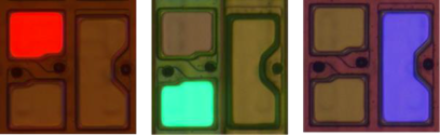
The aperture ratios of the eLEAP OLEDs are shown below which works out to 54.1%.
1.4” eLEAP display with 54% Aperture Ratio
JDI also compared two displays at the same aperture ratio, one with FMMs and the other with eLEAP. The two displays had the same TFT design, same OLED stack, same encapsulation structure, etc. with the same 100% DCI-P3 coverage. They found that the eLEAP panel:
- Showed more stable primary color coordinates over a wider range of display luminance. This was due to lateral carrier leakage in the FMM OLEDs. This causes electrical color mixing, especially at lower luminance values. With eLEAP, because all OLED materials are etched in-between the RGB subpixels, there is no lateral leakage.
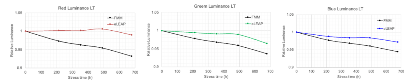
- Showed less color luminance degradation in all three colors despite the same aperture and pixel design. This was attributed to the FMM as a contamination source. When the FMM physically touches the substrate, it can induce a certain amount of impurity into the OLED which can impact lifetime.
Luminance Degradation, 600 nits @35°C
JDI explained that the FMMs are challenging to secure good pixel positions on the mask throughout its tension welding process all the way through the vacuum evaporation chambers, where gravity sagging, thermal expansion and TFT mask alignment errors occur. Because accumulated OLED materials on FMMs thicken the FMM and cause particle generation, FMMs need to be cleaned frequently during mass production which adds to tool downtime and cost.
Using photolithography, sub-pixels can be made larger extending lifetime and suppressing lateral leakage so that low luminance gamma will be smoother, allowing each RGB sub-pixel to have its own optimized materials and thickness, improving OLED device performance. It will also allow for narrower borders, minimizing dark dot growth and scaling to larger OLED sizes without concerns regarding FMM stick width limitations, FMM design leadtimes, FMM costs, FMM cleaning chemicals, etc. JDI has achieved aperture ratios from 27% to 58% and they believe lithography patterning feasibility has been well proven in their prototypes.
Visionox
The Visionox paper was entitled “Development of Visionox intelligent Pixelization (ViP) Technology in AMOLED Applications”.
The Visionox paper also pointed out the downsides of using FMMs:
- The shadow effect and metal etching processes restrict the aperture size, so that >800PPI is not possible;
- Low emitting material utilization;
- Difficult to use MMG to maximize glass utilization;
- Long FMM manufacturing leadtimes and high cost.
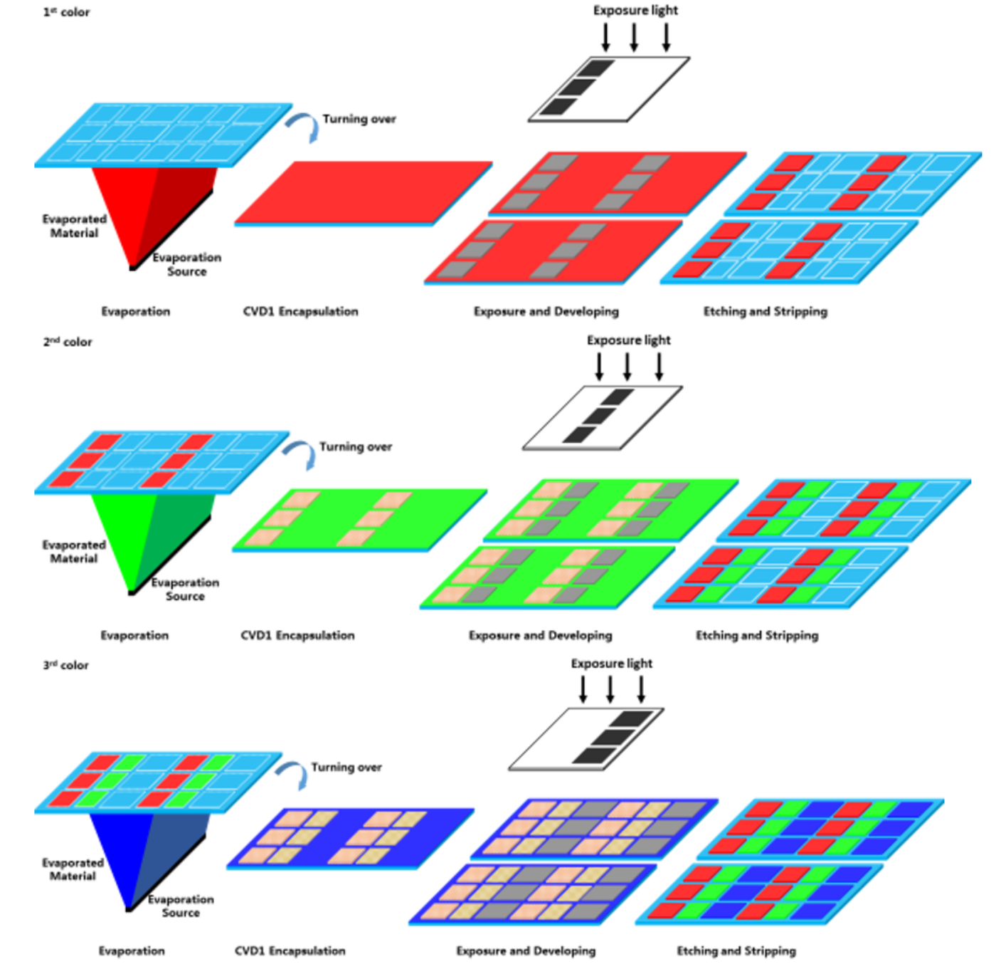
Visionox shared a simplified process of their sub-pixel patterning approach. They pointed out that the color deposition and patterning process can be fully customized based on the electroluminescent device design and other preferences.
ViP Technology
Visionox developed a 7.2” panel with 100% DCI-P3 coverage, a 17um pixel definition layer (PDL) gap and a 29% aperture ratio which it built on its G6 backplane and ½ G6 frontplane line in Hefei (V3).
Visioniox pointed out that the viewing angle performance was improved. Each sub-pixel is completely isolated/independent from each other. The OLED layers, cathode and encapsulation layers can be fully optimized to the desired micro-cavity structure. They claimed this creates a better balance between the device efficiency and the luminance decay. At the same luminance, the power consumption was also reduced by 6.5%.
Better Viewing Angle Characteristics with ViP
Visionox also went into more detail regarding the tunabilty of the stack. In conventional FMMs, the common layers affect each of the sub-pixels with inevitable trade-offs impacting EL optimization. In the case of ViP, each sub-pixel can have their own unique EL structure allowing for optimization of turn-on voltages, operating voltages, capacitance to optimize the performance of each color.
Another benefit is significantly shorter leadtimes for OLED device development. According to Visionox, it is typical to develop blue, then red and green, constrained by materials for the common layers. However, with ViP, all three colors can be developed in parallel, thus shortening new device development times by up to 30% according to their experience.
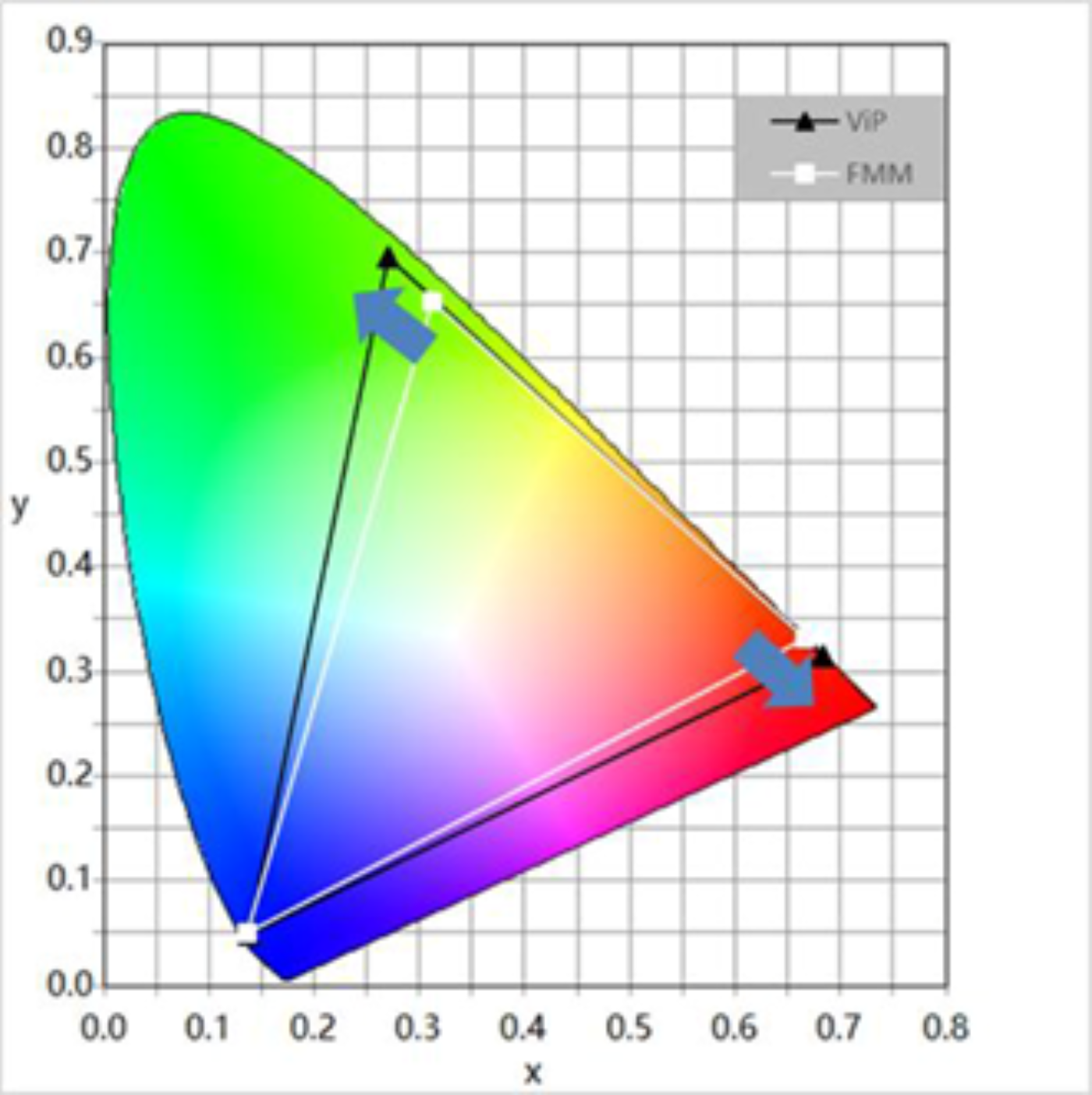
Like JDI, Visionox also pointed out the benefits of complete isolation at the sub-pixel level which completely cuts off cossstalk. As a result, the color gamut coverage at a low grayscale (2 nits at 48 grayscale level for example) can be elevated from about 87% with FMMs to 100% with ViP under simulation. The cut-off of the lateral leakage also further improves the precision of Gamma, so the color rendering at a low gray scale can be optimized.
Improvements in Color Gamut at Low Gray Scale with ViP
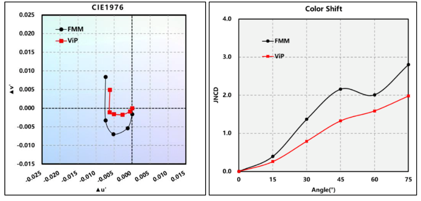
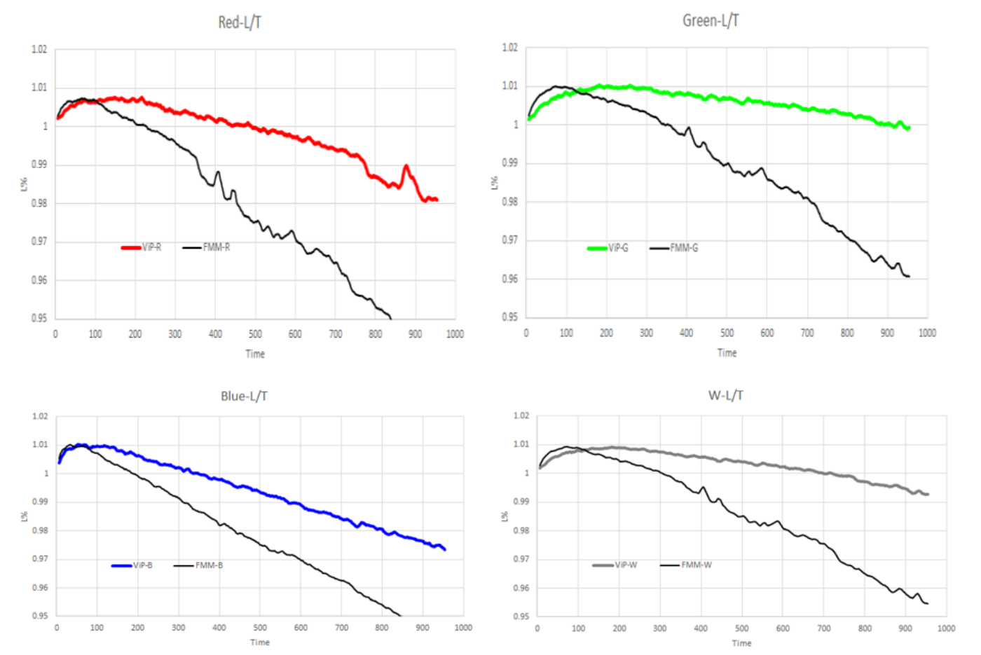
Visionox also pointed out that without the FMM limitations, the PPI limit is defined by photolithography precision and the TFT design requirement. The pixel definition layer (PDL) can easily go down to 10µm and even to 6µm which would enable PPI as high as 1500. While the high PPI can enable new applications like AR/VR, normal PPI with a narrow PDL gap can significantly boost the aperture ratio, extend lifetime and reduce the relevant color shift. Visioniox showed the benefits on lifetime for each color in the following charts.
FMM vs. ViP Color Shift Over Time
Visionox also pointed out that with ViP technology, the input and tracking for the ELVSS signal will be cut by more than 90%, so that issues related to a large IR voltage drop can be solved which include:
- An uneven distribution of ELVSS.
- Requiring buffer of extra voltage during the panel voltage setting.
- Additional IC compensation function to improve the affected luminance and chromaticity uniformity which also consumes extra power.
- Ensuring that different pixel ratios in the same active area will have the same luminance levels.
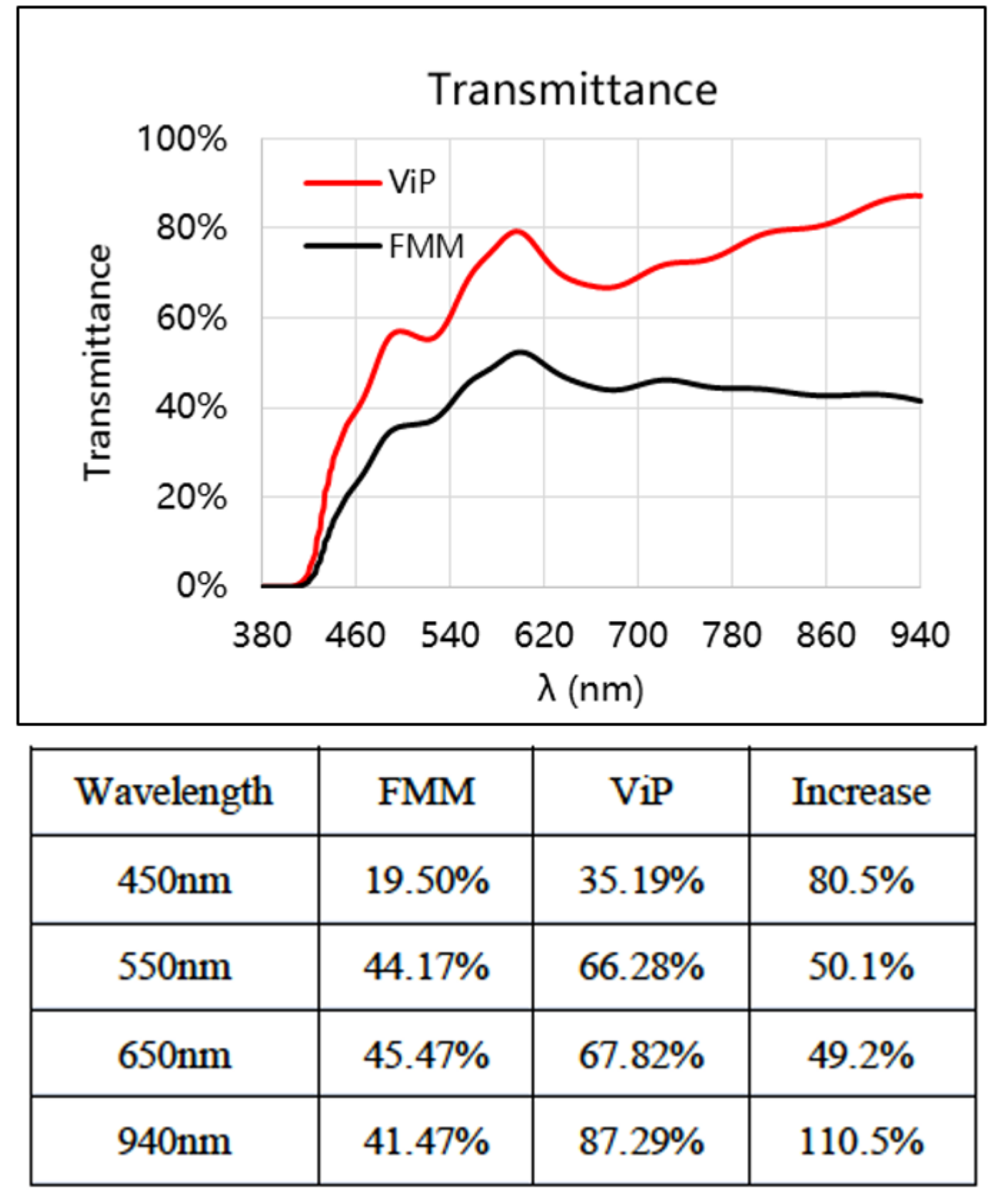
A higher panel transmittance can also improve recognition precision and reduce response times for fingerprint, IR identification and all other under-display sensor performance. A simpler stack can be achieved with CiP in some areas of the pixel with some layers removed such as the cathode. The simulated transmittance of the prototype panel was increased by at least 49% compared with FMM in the visible and IR range. The total panel transmittance was improved from 1.8% with FMM to 3.8% with ViP. The advantage will be more significant at higher resolutions and with CoE panels.
Simulated Transmission Spectra
Visionox concluded that ViP solves all issues related to FMM processes and mask manufacturing and offers:
- Better viewing angle visual performance
- Better low grayscale image quality
- Higher PPI up to 1500 PPI
- Independent EL device design
- Larger aperture ratio and longer lifetime
- Better luminance uniformity
- Lower power consumption
- Lower reliability risk (dark spot growth)
- Higher UV resistance
- Fully customizable shape
- Lower operation cost
- Shorter design leadtime
I think I want one in my next device. Will see when they become available. More on photo patterning OLEDs will be available in our next The Future of OLED Manufacturing Report ※リンク先は2021年版 due out in the fall.