SID/DSCC Business Confarence報告~MicroLEDセッション概要
関連調査レポート MicroLED Display Technology and Market Outlook Report (主筆アナリストのサポートWEB会議付き) の詳細仕様・販売価格・一部実データ付き商品サンプル・WEBご試読は こちらから お問い合わせください。
冒頭部和訳
SID/DSCC Business Conference では複数のバーチャルセッションが実施されたが、そのうちの1つは MicroLEDに焦点を当てたものだった。なお、今年の同セッションではMiniLEDに関するプレゼンテーションはなかった。講演資料集の購入をご希望の方は セミナー事務局 (米国) までご連絡いただきたい。
私 (※DSCCのFPD技術担当ディレクター, Dr. Guillaume Chansin) はMicroLEDのアプリケーション概要と商品化展望について講演した。スマートウォッチはサイズが小さく、ピクセル数が少なく、低価格であることから、MicroLEDアプリケーションとして良いことを説明した。AppleはMicroLEDを搭載したApple Watchの新モデルを2025年に発売すると見られる。LG Displayはバックプレーン用の小規模ラインを構築中で、Osramはマレーシアの新規ラインで8インチウエハーを使用してMicroLEDチップを生産する予定だ。
AUOもQ4’23に1.39インチディスプレイの生産を開始する予定である。AUOは2021年に初めて円形MicroLEDディスプレイのデモを行った。新ディスプレイの解像度は 454×RGB×454 (326 PPI) になると見られる。
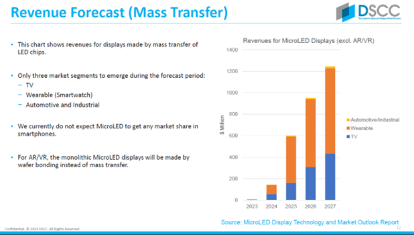
マストランスファー (高速積層) で製造されるMicroLEDディスプレイについては、浮上してきそうなアプリケーションはスマートウォッチ、TV、車載の3つだけだと考えられる。DSCCは現時点ではMicroLEDがスマートフォン市場で多少なりとも市場シェアを獲得するとは予測していない。スマートフォンにはスマートウォッチよりもはるかに多くのピクセル数が必要になるため、LEDチップのコストがはるかに高くなる。ただし、VueRealが最近になってLEDウエハーの消費量を削減するアプローチを開発したことは言及に値する。このアプローチでは、小型サイズのチップとマストランスファーを使用してウエハー使用率を向上させる。VueRealの計算によれば、ウエハー枚数を10分の1以上削減できるという。
AR/VRアプリケーションでは今後、MicroLEDがスマートグラス (シースルーAR) に採用されるだろう。このタイプの MicroLEDはシリコンバックプレーン上に製造されており、マストランスファーによる製造は行われていない。
SID/DSCC Business Conference MicroLED Session Summary
※ご参考※ 無料翻訳ツール (DeepL)
The SID/DSCC Business Conference had several virtual sessions, one of which focused on MicroLED displays. Note that there was no presentation on MiniLED in this session this year. Readers interested in purchasing the recorded SID/DSCC Business Conference proceedings, should contact セミナー事務局 (米国).
I presented an overview of MicroLED applications and the commercialization outlook. I explained that the smart watch is a good application for MicroLED due to the small size, low pixel number and price point. Apple is expected to launch a new model of the Apple Watch with a MicroLED display in 2025. LG Display is building a small line for backplanes and Osram will produce MicroLED chips on 8” wafers in its new fab in Malaysia.
AUO also plans to start production of a 1.39” display in Q4’23. AUO first demonstrated a round MicroLED display back in 2021. The new display is expected to have a resolution of 454 × RGB × 454 (326 PPI).
For MicroLED displays manufactured by mass transfer, only three applications are likely to emerge: Smart watches, TV and automotive. DSCC does not currently expect MicroLED to get any market share in the smartphone market. Smartphones require a lot more pixels than smart watches so the cost of LED chips will be much higher. However, it is worth mentioning that VueReal has recently developed an approach to reduce the consumption of LED wafers. It uses smaller chips and a mass transfer solution that improves wafer utilization. According to VueReal’s calculation, it can reduce the number of wafers by more than 10x.
In AR/VR applications, MicroLED will be adopted in smart glasses (see-through AR). These types of MicroLED displays are made on silicon backplanes and are not manufactured by mass transfer.
David Lewis, CEO of InZiv, talked about the critical need for testing tools. He said that InZiv’s Omnipix tool is sitting in many leading companies developing MicroLED displays today. It is designed for all chip configurations, including flip chip, lateral and vertical. InZiv started selling the system in 2019 and the company now has offices in Israel, Korea and Taiwan.
The Omnipix 2.0 is the current system. It is capable of photoluminescence (PL) and electroluminescence (EL) testing. Optical resolution is down to 100nm. In-wafer EQE testing is also available and is fully automated. Lewis also noted the importance of angular measurement: the tool will not only measure how many photons are emitted, but also where they are going.
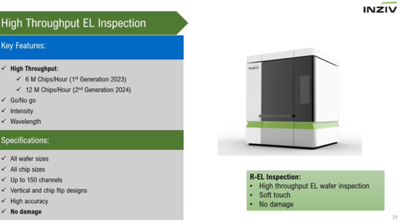
InZiv has also introduced its new tool called R-EL. It is a high throughput EL wafer inspection system. The result is a map with the position of every bad chip on the wafer. It can be done multiple times on the wafer with no damage to the chips. The wafer can be sent to the Omnipix tool for a full report of all the bad chips.
With conventional tools, it can take days if not months to test a complete wafer, but the R-EL will be able to test 6M chips per hour. A second generation system is scheduled for next year will be able to test 12M chips per hour.
Katsumi Araki, Account Manager at Toray Engineering, presented a complete solution for manufacturing MicroLED displays. It includes:
- A non-contact wafer inspection tool (INSPECTRA3000SR);
- A laser trimming tool (LMT-470TR) to remove defective chips;
- A mass transfer tool (MT3000) based on stamp pick and place, with a cycle time of 3s.
Bonding of the chips to the substrate is achieved with a force-sensitive conductive paste from Toray (Raybrid). Another option is to use anisotropic conductive film (ACF) from Dexerials.
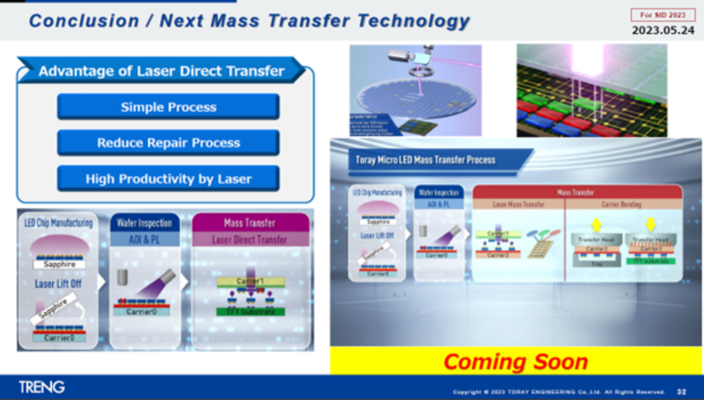
Toray Engineering is currently developing laser mass transfer technology, which will be compatible with larger substrates and offer higher throughput. The company is also working with Advantest to develop another test solution that will enable a faster root cause analysis for yield improvement. The new test solution will collect data of the manufacturing process steps using Advantest’s Cloud Solutions.
David Trasobares Paris, Senior Product Manager at Kulicke & Soffa (K&S), gave a detailed description of the LUMINEX mass transfer technology. It is currently used for MiniLED transfer, but K&S is adapting the materials and process for MicroLED transfer. The company has a business unit for electronic assembly based in the Netherlands.
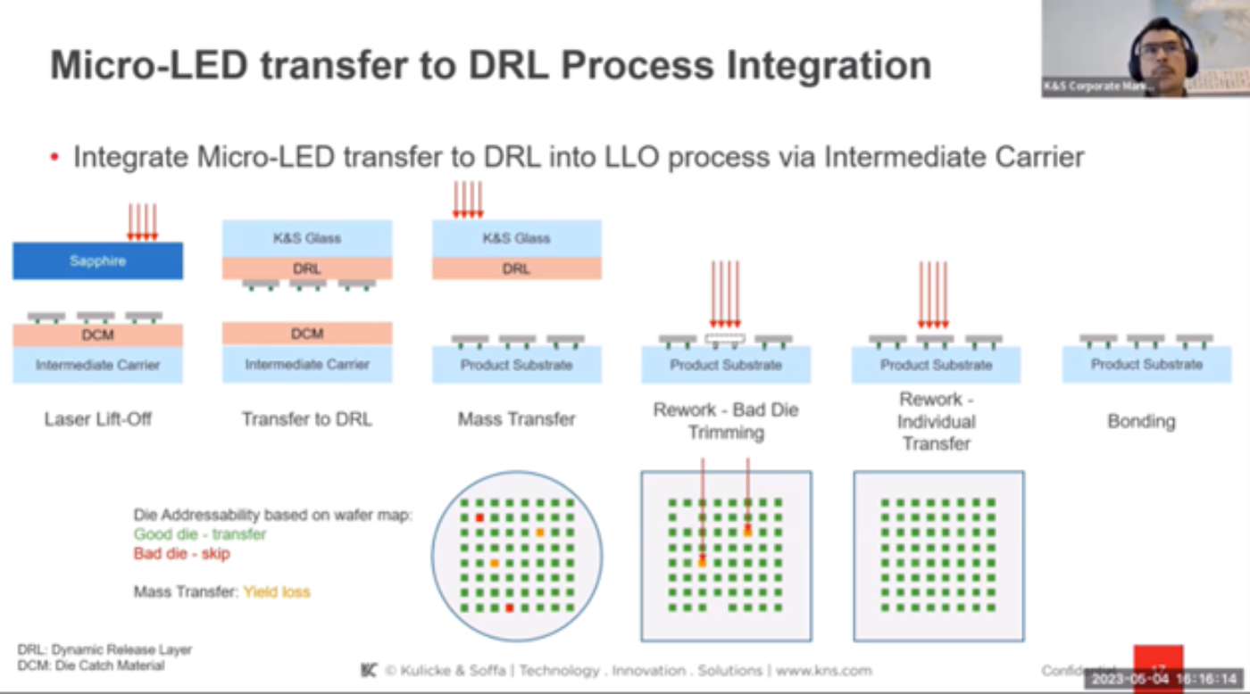
The technology is based on Laser-enabled advanced placement (LEAP). The laser is shot at a dynamic release layer (DRL). This creates a blister that pushes and releases the die in nanoseconds. Placement accuracy is directly related to the die flight distance, so the die should be as close as possible to the substrate before it is released. This is an advantage for MicroLED since the dies are very thin (just a few microns thick), as opposed to MiniLED dies.
K&S uses a diffractive optical element (DOE) for the beam pattern. It means they can adapt to different MicroLED die sizes and shapes. K&S also uses an intermediate carrier, so that the contact pads are in the correct orientation when performing the mass transfer. The company is developing the DRL so that it can support a smaller interspace on the LED wafer, which will help reduce the number of wafers needed. K&S is also looking at various materials for die bonding.
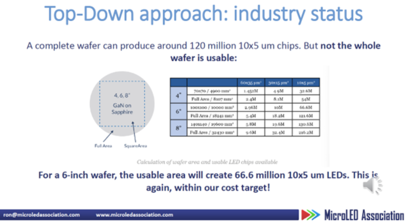
Ron Mertens, CEO of the MicroLED Industry Association explained the fundamentals of yield in MicroLED manufacturing. He then presented a cost analysis that he published in a white paper earlier this year.
For a smart watch, he assumes that the cost for LED chips should not be more than $20. If the resolution is 448 × 368, the cost target is $20 for 494,592 LED chips. He assumes a 150 mm wafer costs $2500 and the usable area is around 16,000 mm2. Combining this with standard LED yields, this gives an area of 235.3 μm2 for each chip. After removing the spacing, he concludes the target chip size should be around 10 μm. He estimates that handling 10x5 μm chips with 5 μm spacing is feasible today.
Art Renn, Special Assistant at Epistar, explained the requirements for MicroLED commercialization:
- Good wavelength uniformity, with deviation less than the just noticeable color difference (JNCD);
- Defect level after the first pass should be 50ppm or less (99.995% yield), either with chip on glass (COG) or chip on board (COB);
- The price should be competitive with OLED TV.
Epistar is part of the Ennostar group. Epistar is specialized in epitaxy and chip processing, while Lextar focuses on packaging and modules. Unikorn is an 8” GaN on Silicon foundry for power components and MicroLEDs.
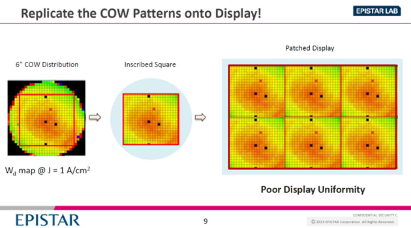
Chips on wafer (COW) will always exhibit non uniformity. Large patterns on the wafer will be replicated after mass transfer, which will lead to mura.
Uniformity must be measured for any current density that will be used to produce gray levels in the final displays. Epistar’s solution is then to repopulate dies to a carrier, in such a way that there is no visible pattern. Epistar also removes defective dies in the process: this helps achieve a first pass yield of 99.995% and no repair is necessary.
Epistar can also place the dies at the correct pixel pitch so that they are ready for mass transfer. They call it “Spatial COC” and it is available in monochrome or color (with three subpixels).
----------------------------------
関連調査レポート MicroLED Display Technology and Market Outlook Report (主筆アナリストのサポートWEB会議付き) の詳細仕様・販売価格・一部実データ付き商品サンプル・WEBご試読は こちらから お問い合わせください。