SID/DSCC 2022ハイライト~MiniLEDとMicroLED動向
Summary of the MiniLED and MicroLED Session at the SID/DSCC Business Conference
One of the virtual sessions at the SID/DSCC Business Conference was dedicated to advances in MicroLED and MiniLED. This article presents the highlights from this session. You can still register to watch all recordings of the conference.
DSCC
Leo Liu opened his talk with an observation that the Haitz Law held from the 1960s through the 2020s and appears to be on track for the 2030s. Haitz Law is considered to be the equivalent of Moore’s Law for the LED industry. It states that after each decade, the amount of Lumen per package increases by 20× and the cost per Lumen decreased by 10×.
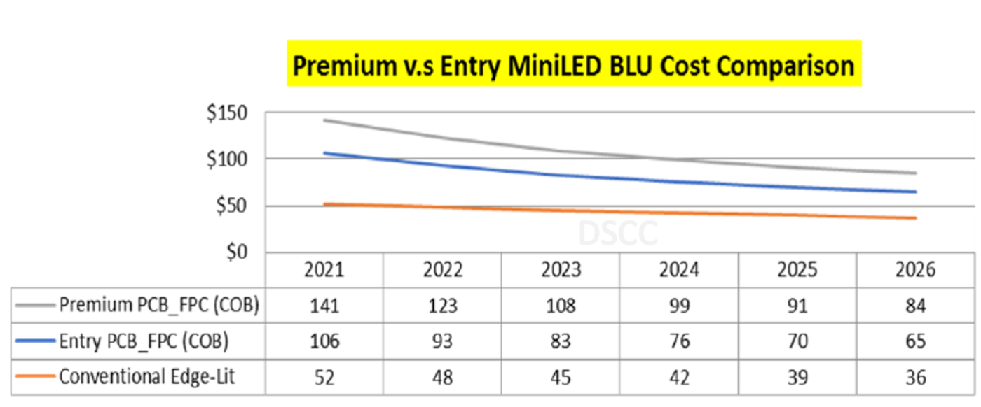
However, a MiniLED BLU can use thousands of LED chips, so the total chip area is much higher than with a conventional edge-lit BLU. This is why panel makers are also offering entry-level MiniLED solutions with fewer LED chips and dimming zones.
Following the iPad Pro, Apple has successfully introduced MiniLED to the MacBook Pro. Over 2M MacBook Pros were shipped in Q1 this year. MiniLED has become an alternative to OLED for premium notebooks. Apple products will represent a large share of MiniLED tablets and notebooks at least until 2025.
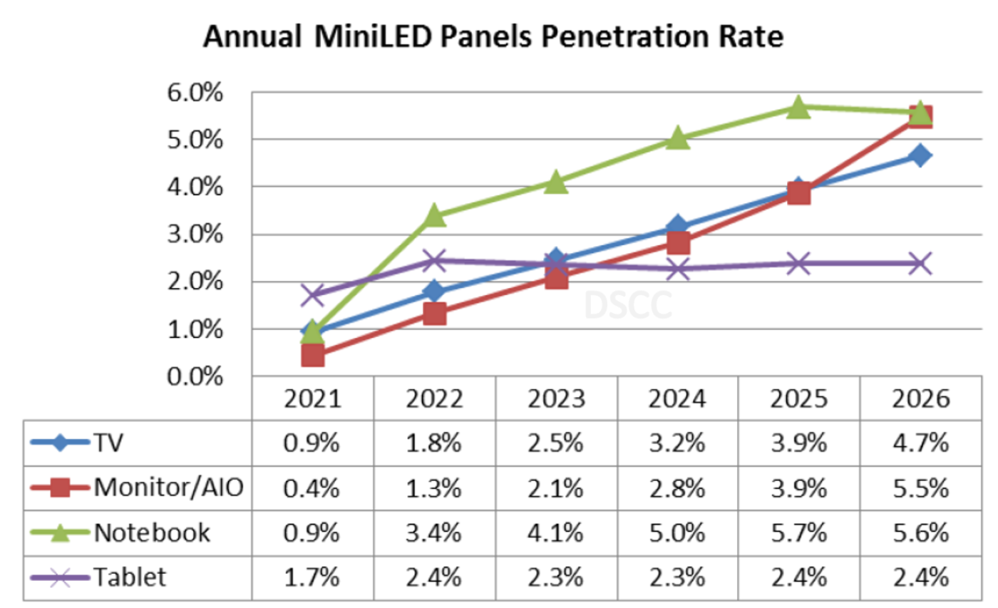
In notebooks, MiniLED will gain market share until 2025 but the penetration rate will start to drop after 2026 due to the competition from OLED. For large-size panel (monitor and TV), the penetration of MiniLED looks more promising than tablet and notebook. Samsung, LG and main TV brands in China keep pushing MiniLED TV to market. This will drive TV to become the largest application for MiniLED shipments after 2026.
SmartKem
Ian Jenks, Chairman and CEO of SmartKem, did not talk specifically about MiniLED and MicroLED but gave an overview of what is possible now with organic TFT. SmartKem raised $24.6M last year through a private placement of common stock. The company is now working with Nanosys on “a variety of applications” which include MicroLED.
Their OTFT can be processed at a temperature as low as 80°C. They have scaled up to Gen2 (370mm × 470mm) glass or flex substrates in their UK facilities and are currently engaging with a partner in Asia to qualify the world’s first OTFT roll-to-roll process.
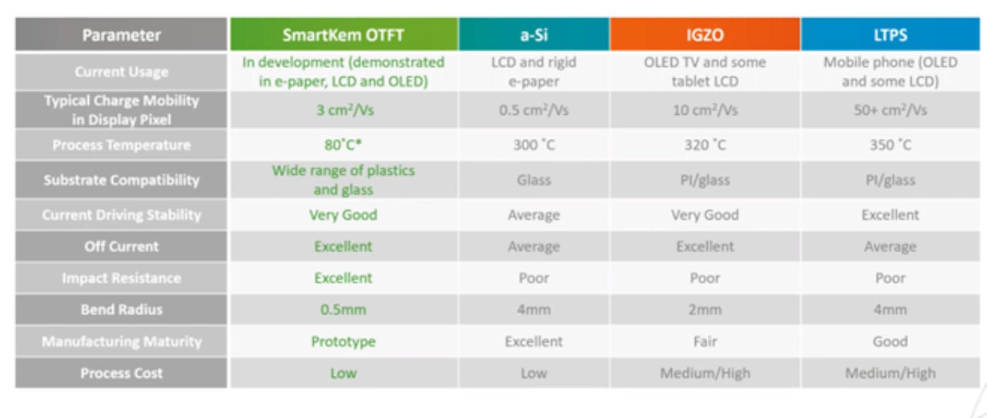
According to SmartKem, OTFT can now be used to replace some silicon ICs. The conventional knowledge is that ICs require CMOS inverter logic, using both PMOS and NMOS transistors. The problem with OTFT is that they are only PMOS. It means that noise margin and gain is lower than for CMOS. However, it is possible to design a pseudo CMOS circuit with one type of transistor.
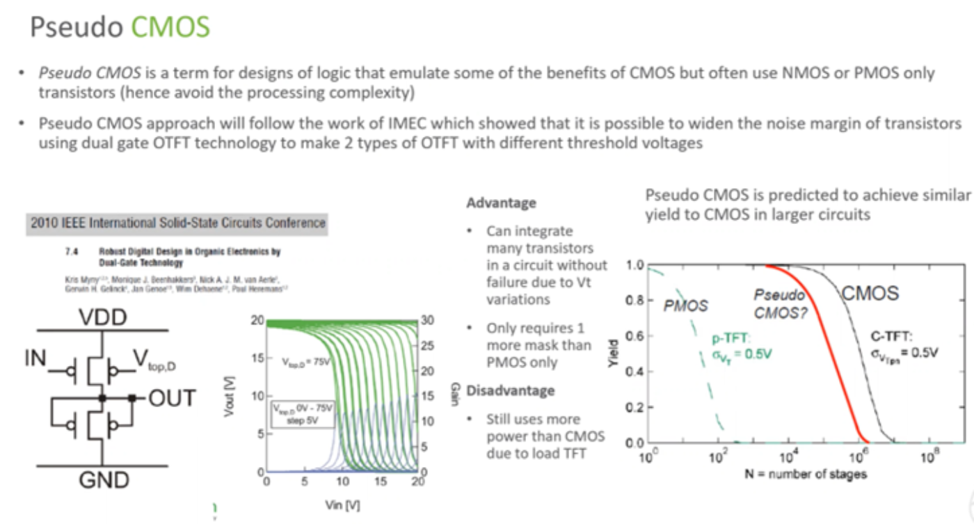
Using dual gate inverters, SmartKem says OTFT could be used for display gate-on-array and other type of driving circuitry (not source driver). The company has achieved a mobility above 2 cm2/Vs for all channel lengths. The normalized contact resistance is typically below 200 Ohm.cm.
SmartKem is also working on AMOLED displays. It has a JDA with RiTdisplay to collaborate on the production of a full color AMOLED display using OTFT backplanes that integrate shift register and mux-demux functionalities.
Rohinni
Justin Wendt, CTO of Rohinni, said that the definition of what a MicroLED is, has changed in recent years. Chips that were bigger than 100 μm used to be labelled as MicroLED but they are now commonly defined as MiniLED.
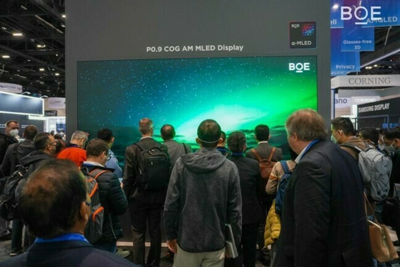
He added that Rohinni provided the placement technology behind the active-matrix glass display that BOE was showing in the exhibition. The BOE booth had a large emissive LED display based on chip-on-glass (COG) technology and a pixel pitch of 0.9mm. BOE also won the Display Components of the Year award for its 86” COG MiniLED backlight unit.
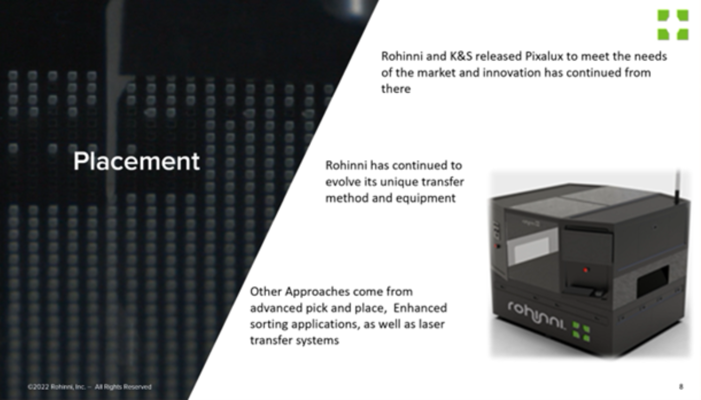
One benefit of using glass substrates is that the additive sputtering process can be layered to create much more accurate and cleanly defined contact pads (so glass is more suited to smaller LED chips). The placement technology is designed for LEDs as well as driver ICs and offers a component yield of 5N (99.999%).
The focus today is on packing as many emitters as possible into the smallest area, for as cheap as possible. Justin Wendt acknowledged that laser mass transfer technologies have recently emerged, operating faster than a mechanical transfer. However, for large arrays the substrate alignment will be the main bottleneck of a laser-based transfer.
Mojo Vision
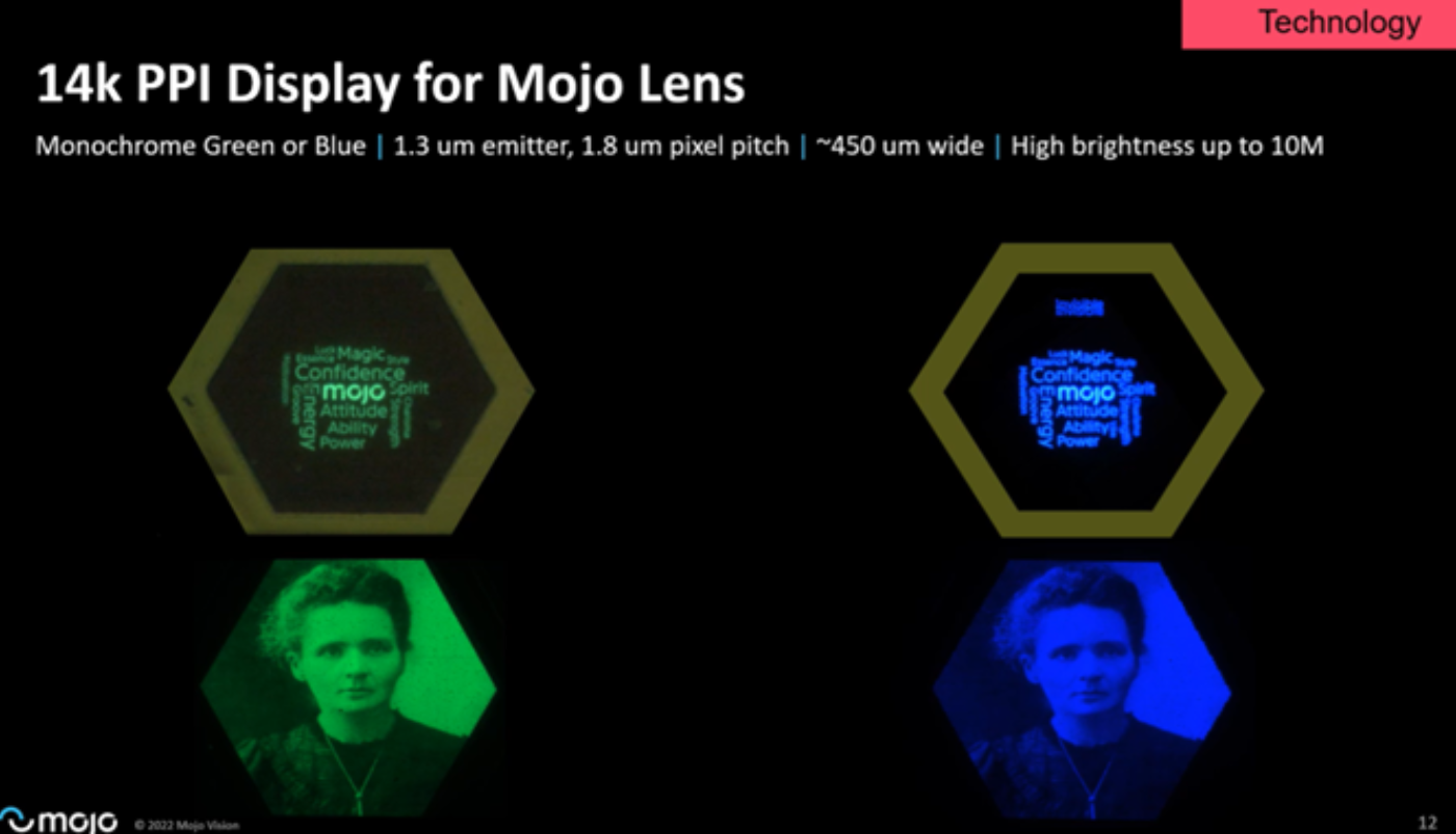
Dr. Nikhil Balram, SVP and GM Displays at Mojo Vision, started by introducing Mojo Lens, the first AR contact lens. The development of this product required the creation of the world’s smallest and densest MicroLED display. It measures approximately 0.45mm. Mojo Vision is now aiming to develop a MicroLED display business for other applications. The message is that MicroLED will eventually take over the entire display market, like LCDs did from CRT.
According to Mojo, the most meaningful segmentation of the MicroLED display market is by density. On one hand, dense displays start at ~2500 PPI and can reach up to 15,000 PPI. This includes augmented reality (AR) light engines and lightfield displays. On the other hand, sparse displays have a density of 1000 PPI or less.
Mojo believes that some MicroLED companies (group A) are able to do very small emitters using new semiconductor technologies, while others (group B) can only do larger size emitters. The idea is that companies in group A can first enter the market through AR applications and later address sparse displays.
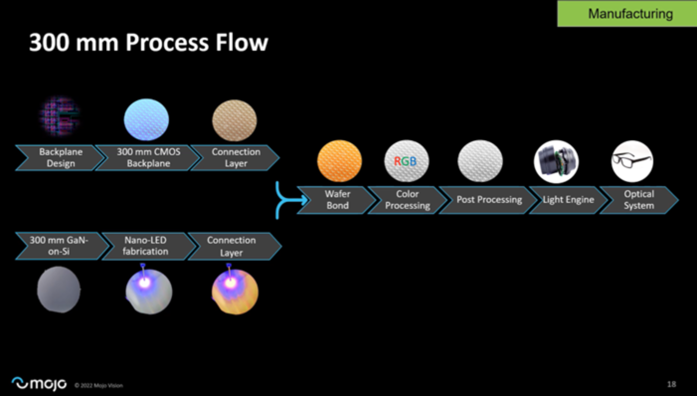
Mojo says it has a unique core MicroLED technology for efficient small emitters and a proprietary RGB process. The company also has expertise in CMOS backplane design, bonding/packaging and optics (for emission control). They use GaN on silicon and the manufacturing is based 300mm wafer to wafer bonding, which is suitable for volume manufacturing.
Mojo is working on backplane architecture for AR and other markets. The current CMOS backplane is designed specifically for the Mojo Lens and offers several features to keep power consumption low:
- Random access (only the pixels that are “on” are sent to the display);
- Constant current source;
- Brightness control via PAM, PWM and TDM to support a wide intensity range.
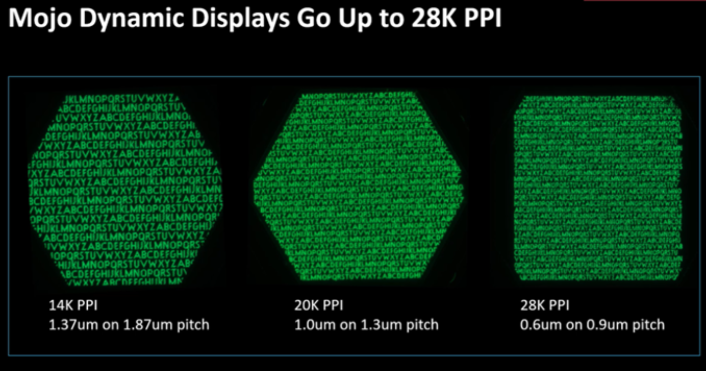
The display for Mojo Lens is 14K PPI but the company has also demonstrated 20K PPI with ~1% dim/dead pixels. They also have a 28K PPI display in development.
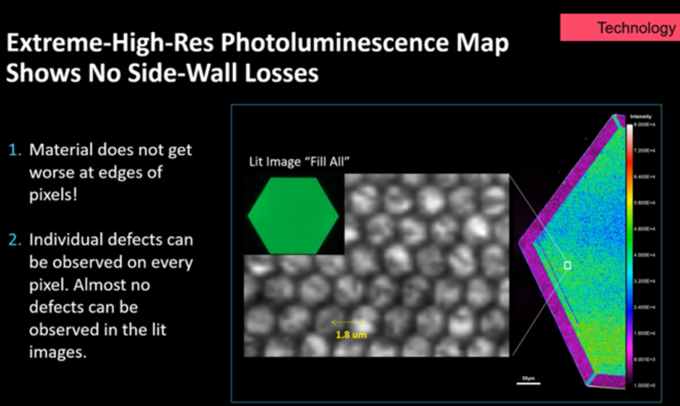
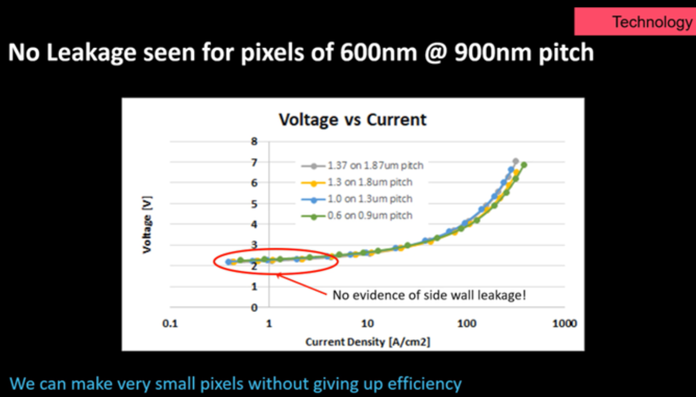
Mojo has optimized its pixel architecture to prevent side-wall losses and side-wall leakage. The company is now looking for long-term strategic customers, investors and partners.
Porotech
Dr. Tongtong Zhu, CEO of Porotech, introduced the company’s PoroGaN platform as an interplay between material design, fabrication and device integration. It enables all three primary colors to be generated with a single material system: Indium Gallium Nitride (InGaN). The company believes MicroLED displays based on PoroGaN are ideally suited for the next generation of XR, near-eye applications, wearables, TVs and other consumer electronics devices.
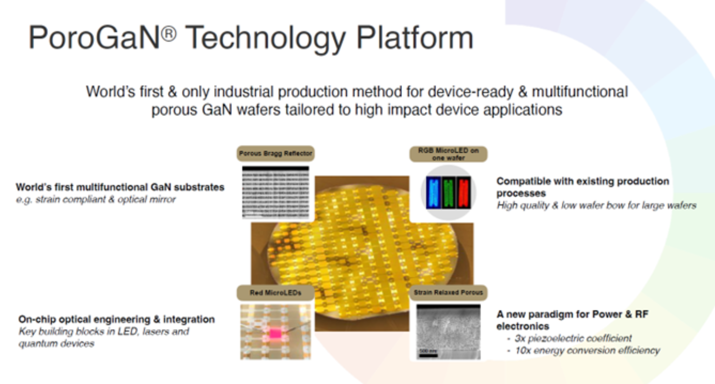
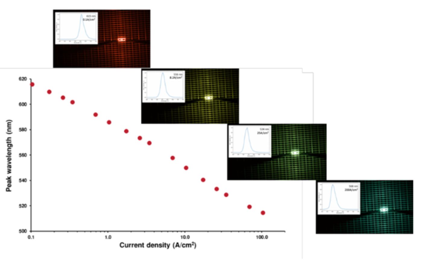
For red color, there is a significant lattice mismatch which makes it particularly tricky to increase the amount of indium in the composition. Native red with InGaN has been investigated by others using either nanowire LEDs or strain-relaxed substrates. Porotech uses the porosity of its material to incorporate more indium in quantum wells. The porosity also reduces wafer bow, an important parameter for epitaxy but also for wafer bonding.
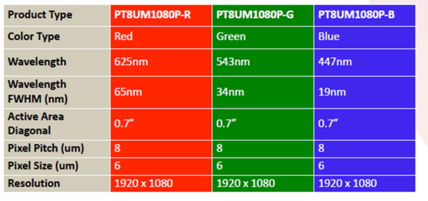
Porotech is now offering 0.7” monochrome microdisplays with Full HD resolution. The pixel density is 3000 PPI and the brightness is at least 2M nits. Dr Zhu said that they have not removed the sapphire substrate on the current prototypes. With the proper light extraction optimization (beam shaping), he believes that luminance over 20M nits is possible.
The presentation did not include data on the DynamicPixelTuning technology, as the recording was submitted before the official announcement. However, a graph included in the PDF shows how the emission wavelength is shifted by varying the current density over a wide range. The company does not specify how the EQE is impacted.