Future of OLED Manufacturing Report 最新版を近日発刊~将来のIT/モバイル/TV向けOLED製造における主要リスク/課題/期待されるソリューションが明らかに
出典調査レポート Future of OLED Manufacturing Report の詳細仕様・販売価格・一部実データ付き商品サンプル・WEB無料ご試読は こちらから お問い合わせください。
これらDSCC Japan発の分析記事をいち早く無料配信するメールマガジンにぜひご登録ください。ご登録者様ならではの優先特典もご用意しています。【簡単ご登録は こちらから 】
DSCC’s Upcoming Future of OLED Manufacturing Report Reveals Key Risks, Challenges and Expected Solutions in Future IT, Mobile and TV Production
※ご参考※ 無料翻訳ツール (DeepL)
DSCC's Future of OLED Manufacturing Report will be released shortly and includes detailed analysis and insights on how OLED panels and manufacturing are likely to evolve as the market expands. It examines:
- How the TFT backplane will likely change at G8.7;
- How the OLED frontplane will change at G8.7;
- How OLED materials are evolving and how they are likely to be commercialized;
- All the different approaches OLED manufacturers are taking to boost efficiency and/or lower power consumption;
- How smartphone panel manufacturing will change;
- How OLED TV panel manufacturing is expected to change;
- And much more.
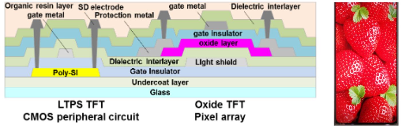
For example, we go into great depth regarding the risks, challenges and solutions for high mobility oxide TFT and LTPO backplanes for G8.7. We reveal a somewhat new backplane approach that a leading customer has proposed called LTPO+. In this approach, the array would be made with oxide TFTs, but the edges of the display, where the driving and multiplexing circuitry would be located which requires higher mobility and stability, would be LTPS. JDI actually proposed this for LCDs in 2019 and some prototypes were made as a way to lower power consumption. JDI called it Advanced LTPS TFT Technology and produced CMOS LTPS TFTs for the driver area with mobilities of 66cm2/Vs for N channel TFTs and 90 cm2/Vs for P channel TFTs with the oxide TFT array having 9.5cm2/Vs mobilities and excellent mobility results. The refresh rate was reduced to 5Hz for the array and the edge borders were 0.6mm.
LTPO+ Backplanes
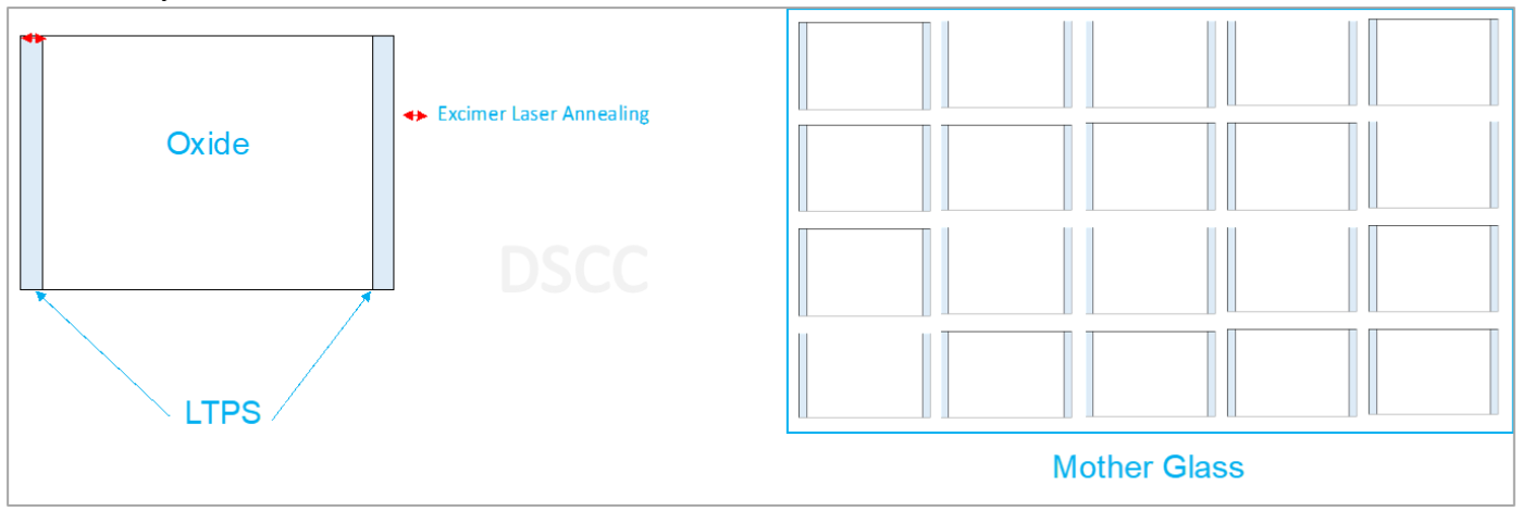
JDI’s Advanced LTPS TFT Structure
Selective annealing has been proposed before, most notably by SLS technology pioneered by Dr. James Im from Columbia University. We believe the reason this structure is being proposed for future G8.7 fabs is due to the challenges associated with high mobility oxide TFTs and the desire to expand multi-sourcing. It is difficult to manufacture oxide TFTs with both high mobility and high stability. Producing higher mobility TFTs often involves narrowing the process window and can involve greater complexity as well, reducing the capex advantage over LTPS and LTPO. Higher mobilities enable smaller transistors with greater current capability, faster switching speeds and higher frame rates, higher circuit integration and narrower bezels and lower power. Thus, higher mobilities and excellent stability will be required if oxide is going to replace LTPS/LTPO in IT markets.
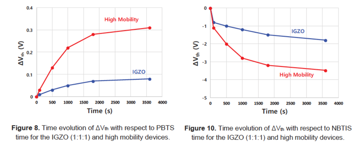
However, as SDC revealed in their 2022 paper Development of High Performance IGZO Backplanes for Displays published by SID in 2022, “High mobility devices are more sensitive to the fabrication process, most notably regarding hydrogen incorporation and undergo relatively large Vth shifts under both positive bias temperature stress (PBTS) and negative bias temperature stress (NBTS)” as shown in the figures below. How to overcome this problem will be important for panel manufacturers. In addition, whether all manufacturers can solve this challenge in the same timeframe is also a concern for customers to enable multi-sourcing with reasonably similar panel performance. Thus, the LTPO+ backplane is a way for customers to reduce their risk as panel manufacturers can more easily produce an oxide TFT with good stability at lower mobilities and can deposit LTPS where higher mobilities are needed. However, it will likely result in higher costs vs. an all oxide TFT panel if it could meet the mobility/bezel width/uniformity requirements. The report delves into all the different approaches panel manufacturers are taking to solve high mobility, desired stability issues including alternative device architectures, different oxide and other materials, process optimization along with reported metrics and which approach has the best potential to meet the performance and cost targets.
High Mobility IGZO vs. Traditional IGZO Stability Results
Another area of interest is high efficiency blue OLED emitters. This report examines the approach leading OLED manufacturers are taking towards commercializing high efficiency blue OLED emitters. In the case of one manufacturer, we report on four different paths covering two different applications along with the lifespan and efficiency status and targets for commercialization along with their anticipated commercialization timing. We also report on other ways leading manufacturers are able to achieve higher performance while also reducing cost or minimizing the cost increase. For example, we explain through one manufacturers’ roadmap how the number of additional masks for color on encapsulation or POL-LESS will fall by more than 1/2. We also report on panel suppliers’ tandem roadmaps for power and brightness, the biggest challenges for tandem TFTs and the steps panel manufacturers are taking to overcome these challenges.
Other areas covered in detail include:
- Micro OLED Manufacturing Challenges, Device Structures, Roadmap, Capacity Forecasts, Shipment Forecasts and More
- Low Frequency LTPS TFTs
- Other Power Saving Techniques
- Double Capping Layers
- Photo Patterning OLEDs vs. FMM OLEDs
- OLED Glass Thinning
- Under Panel Cameras
- Under Panel Face ID
- MLA/MLP
- Burn-In
- Fab Schedules
- Capex Comparisons
出典調査レポート Future of OLED Manufacturing Report の詳細仕様・販売価格・一部実データ付き商品サンプル・WEB無料ご試読は こちらから お問い合わせください。
[12/28追記] 目次速報
第1章 Executive Summary
第2章 Background – OLED Status
2.1 Revenues, Share of Display Market by Application
2.2 Units, Share of Display Market by Application
2.3 Supplier Share
2.4 Fab Schedule Forecast and Capex
2.5 OLED Capacity Forecast
第3章 Technical Challenges and Bottlenecks for OLEDs
3.1 Known Historical Production Challenges
3.2 Current OLED Yield Challenges
3.3 Current OLED Material Challenges
3.4 OLED’s Cost Challenge
3.5 Micro OLED Yield and Cost Challenges
第4章 OLEDs in Smartphones and Wearables
4.1 Overview and Latest Forecast
4.2 Low Frequency LTPS and Other Power Saving Developments
4.3 LTPO
4.4 Color on Encapsulation
4.5 Micro Lens Arrays/Patterns
4.6 Apple’s iPhone Roadmap
4.7 Under Panel Cameras and IR Sensors
4.8 High Resolution Lithography and Maskless Lithography
4.9 Mobile OLED Stacks
4.10 Deuterium
4.11 Double CPL and Patterned CPL
4.12 High Efficiency Blue OLED Emitters
4.13 Plasmonics
4.14 Foldables and Rollables
第5章 OLEDs in IT
5.1 The IT Opportunity and Apple’s IT OLED Roadmap
5.2 Current OLED Notebooks, Tablets and Monitors
5.3 The Challenge/Problem and Panel Requirements
5.4 G8.7 IT OLED Backplane Challenges
5.4.1 Scaling LTPO
5.4.2 Oxide and LTPO+
5.4.3 High Mobility Oxide Benefits and How to Boost Mobilities
5.4.4 High Mobility Oxide Challenges and Solutions
5.4.5 Glass Thinning
5.5 G8.7 IT OLED Frontplane Challenges
5.6 Alternative Patterning Approaches
5.7 Tandem Stacks – Benefits and Challenges
第6章 OLEDs in TVs
6.1 Overview
6.2 WOLED
6.3 QD-OLED
6.4 OVJP Status
6.5 IJP RGB OLED Status
6.6 High Efficiency Blue for TVs
6.7 Auxiliary Electrodes
6.8 Cost and Shipment Forecasts
第7章 OLEDs in AR/VR
7.1 Why Micro OLED for AR/VR?
7.2 Fab Schedules and Capacity
7.3 Supply Chain
7.4 Performance and Design Requirements
7.5 WOLED with Single and Tandem Stacks
7.6 Direct Patterning
7.7 Micro OLED Architecture with MLA
7.8 Micro OLED Forecasts
出典調査レポート Future of OLED Manufacturing Report の詳細仕様・販売価格・一部実データ付き商品サンプル・WEB無料ご試読は こちらから お問い合わせください。